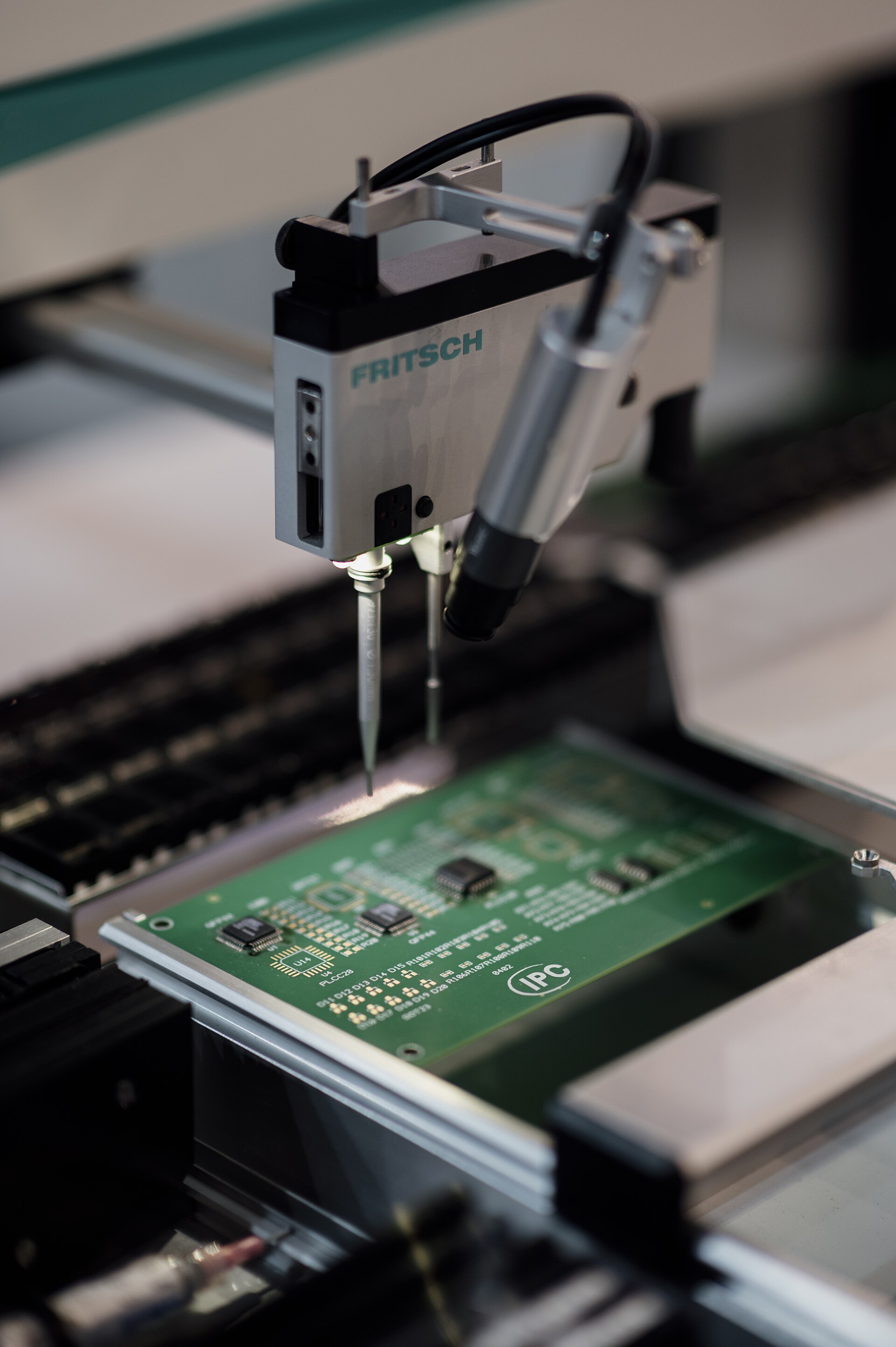
Engineering review
Production begins with a review of Gerber files, drill files, netlist, stackup, material, copper weight, board thickness, surface finish and special notes. Engineering review confirms whether the design can be manufactured consistently.
Material preparation
The selected laminate and copper foil are prepared according to board thickness, layer structure and application requirements. Material choice affects thermal reliability, dimensional stability and electrical performance.
Inner layer processing
For multilayer PCB, inner copper layers are imaged, etched and inspected before lamination. AOI is commonly used to find opens, shorts or registration issues before the layers are pressed together.
Lamination
Inner layers, prepreg and copper foil are aligned and laminated under controlled heat and pressure. Lamination quality influences layer registration, thickness and long-term reliability.
Drilling and plating
Mechanical or laser drilling creates holes and vias. Plating builds conductive copper through the holes and across surfaces, enabling electrical interconnection between layers.
Imaging and surface finish
Outer layers are patterned, etched and protected with solder mask. Surface finishes such as HASL, Lead Free HASL, ENIG and OSP are selected according to assembly and application requirements.
Testing
Electrical testing, AOI, visual inspection and final checks confirm that the PCB meets the manufacturing data and quality requirements before shipment.