Manufacturing capability
Process coverage includes inner layer imaging, lamination, drilling, plating, solder mask, surface finish and routing for multilayer builds.
Multilayer PCB
YBCPCB supports multilayer PCB fabrication where routing density, lamination quality, stackup planning and inspection discipline are important.
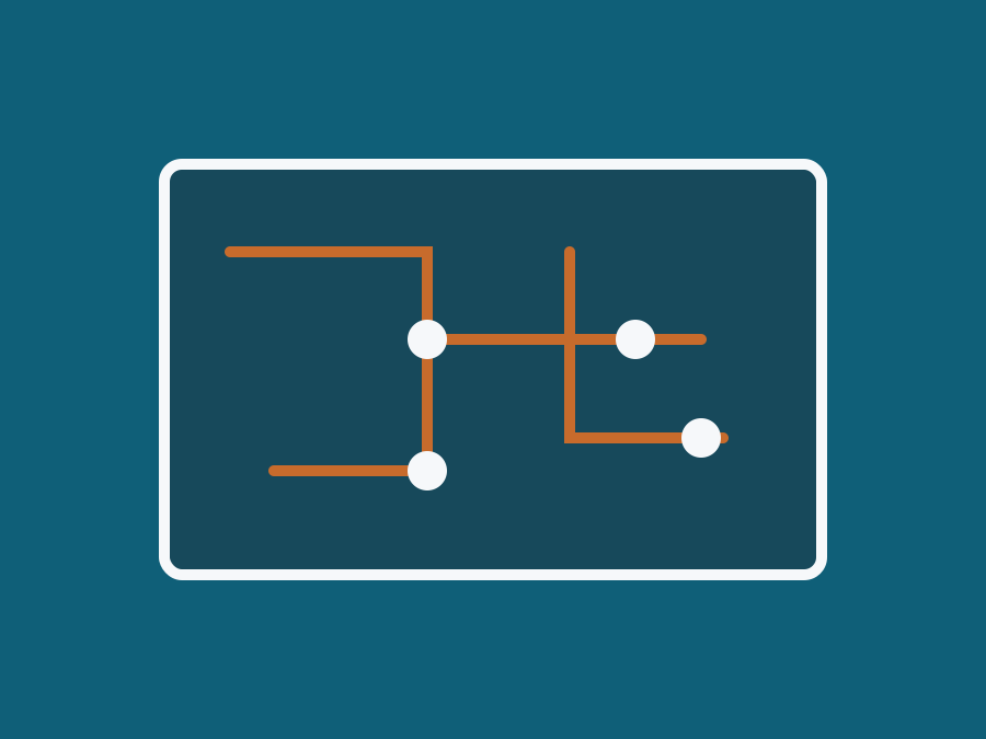

A multilayer PCB uses three or more conductive copper layers laminated together with insulating material. It allows more routing space, better power distribution and cleaner signal organization than simple two-layer boards.
YBCPCB helps overseas customers review material, stackup, impedance and manufacturing notes before production.
| Specification | Typical support | Buyer note |
|---|---|---|
| Layer count | 4 layer, 6 layer and additional multilayer builds by review | Include stackup and impedance notes if available |
| Material | FR4, high Tg FR4 and selected laminate options | Thermal and signal needs affect material choice |
| Drilling | Through-hole drilling and plated through holes | Share minimum hole and annular ring requirements |
| Testing | Electrical test and final inspection | Recommended for prototype and production orders |
Product Visuals
Visual content helps buyers connect product capability with real PCB fabrication steps and quality control.

| Technical parameter | Manufacturing review |
|---|---|
| Layer capability | 2-32 layers by stackup, drill and board thickness review |
| Materials | FR-4, High Tg, Halogen Free and selected laminate options |
| Surface finish | HASL, Lead Free HASL, ENIG, OSP and Immersion Silver by application |
| Inspection | AOI, electrical testing and final visual inspection |
Process coverage includes inner layer imaging, lamination, drilling, plating, solder mask, surface finish and routing for multilayer builds.
IoT gateways, motor controllers, measurement equipment, network hardware, power management and medical device electronics.
Multilayer PCB can improve routing density, reduce board size, support better grounding and organize power distribution more effectively.
It is useful when routing density, board size, power integrity or signal organization cannot be handled well on a two-layer PCB.
Yes, if your design has impedance, thickness, dielectric or controlled stackup requirements.
Yes. Multilayer prototype PCB orders help validate complex designs before production.
Engineering Review
This PCB product page supports buyer review with manufacturing capability, applications, advantages, FAQ guidance and related engineering pages.
Review layer count, board thickness, copper weight, material, surface finish, solder mask and inspection requirements with complete files.
Industrial electronics, medical accessories, automotive modules, IoT hardware, consumer devices and power control boards by project review.
Structured file review helps align manufacturability, quality checkpoints, application requirements and production planning.
| FAQ item | Engineering answer | Related page |
|---|---|---|
| What files should be sent? | Gerber files, drill files, board outline, stackup notes, material and finish requirements. | File guide |
| How is feasibility reviewed? | Engineering checks stackup, trace and spacing, drilling, copper, surface finish and quality requirements. | Capabilities |
| Which related topics help selection? | Technology comparison, materials, stackup design, via types and quality control can guide early decisions. | Technology comparison |
Include stackup, material and tolerance notes for engineering review.